
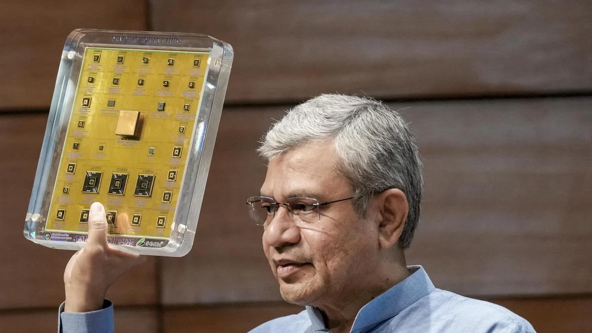
In a landmark move poised to redefine India’s industrial landscape, the Union Cabinet on July 15 cleared the second phase of the India Semiconductor Mission (ISM) and simultaneously launched the Mobile Phone Manufacturing Scheme (MPMS). With a monumental outlay of ₹1.27 lakh crore for ISM and ₹62,500 crore for MPMS, these programmes signal India’s resolute commitment to achieving technological self-reliance and asserting its position in the global electronics value chain. This ambitious dual thrust aims to cultivate a robust domestic ecosystem for semiconductor fabrication, assembly, and packaging, alongside fostering indigenous mobile phone assembly and component manufacturing. The government anticipates these schemes will catalyze a staggering ₹4 lakh crore in investment, generate ₹2 lakh crore in production value, and fuel ₹1 lakh crore in exports over their five-year tenure, marking a pivotal chapter in India’s journey towards becoming a global manufacturing hub.
Main Facts: India’s Ambitious Leap into High-Tech Manufacturing
The recent Union Cabinet approval of the second phase of the India Semiconductor Mission (ISM) and the Mobile Phone Manufacturing Scheme (MPMS) represents a strategic pivot in India’s industrial policy, emphasizing high-tech manufacturing and critical component production. This comprehensive initiative, backed by substantial financial commitments, seeks to build an indigenous ecosystem for crucial electronic components, reducing reliance on volatile global supply chains.
A New Era of Incentives
The core of this new policy thrust lies in its impressive financial commitments and ambitious targets. The India Semiconductor Mission (ISM) Phase 2 has been allocated a significant outlay of ₹1.27 lakh crore, designed to attract and support advanced semiconductor fabrication, assembly, and packaging units within the country. This funding is crucial for an industry characterized by its capital-intensive nature and rapid technological evolution. Simultaneously, the Mobile Phone Manufacturing Scheme (MPMS) has been endowed with ₹62,500 crore, specifically aimed at bolstering domestic mobile phone assembly capabilities and, more importantly, incentivizing local component manufacturing and design.
The government’s projections for these schemes underscore their transformative potential. Over the next five years, these initiatives are expected to draw an estimated ₹4 lakh crore in fresh investments across the semiconductor and mobile manufacturing sectors. This influx of capital is anticipated to translate into a production value of ₹2 lakh crore, with a significant portion, ₹1 lakh crore, earmarked for exports. These figures are not merely economic targets; they represent a strategic vision to integrate India more deeply into global electronics value chains, enhance its manufacturing prowess, and establish it as a reliable and competitive player in the high-tech arena. The dual focus on semiconductors—the bedrock of modern electronics—and mobile phones—a ubiquitous consumer device with immense market potential—highlights a calculated approach to building a diversified and resilient electronics manufacturing base.
Chronology: Tracing India’s Semiconductor Journey
India’s journey towards establishing a robust semiconductor and electronics manufacturing ecosystem is not new but has gained unprecedented momentum in recent years. The latest announcements build upon foundational policies and lessons learned from previous initiatives, signifying an evolving and increasingly sophisticated approach.
The Genesis: ISM Phase 1 (December 2021)
The first significant stride in this direction was taken in December 2021, with the initial approval of the India Semiconductor Mission (ISM) Phase 1. This inaugural phase was launched with an outlay of ₹76,000 crore, signaling the government’s recognition of semiconductors as a strategic industry. The primary objective then was to attract major investments into semiconductor fabrication, display manufacturing, and design.
A crucial amendment in 2022 significantly enhanced the attractiveness of ISM Phase 1. This amendment empowered the programme to provide capital subsidies of up to 50% for large-scale, high-investment projects. This enhanced incentive proved instrumental in drawing global players to India, notably culminating in Micron Technology’s decision to establish a memory chip packaging facility in Sanand, Gujarat. This facility, a cornerstone of India’s nascent semiconductor ambition, stands as a tangible outcome of the first phase’s strategic adjustments. Furthermore, the funds from ISM Phase 1 were also directed towards the Electronics Component Manufacturing Scheme (ECMS), designed to incentivize the production of smaller yet critical electronic components, thereby laying the groundwork for a broader manufacturing base. The initial phase, while a learning curve, successfully planted the seeds for larger aspirations.
Evolving Ambitions: The Shift to ISM Phase 2 (July 202X)
The recent Cabinet clearance on July 15 for ISM Phase 2 marks a maturation of India’s semiconductor strategy. The interval between Phase 1 and Phase 2 has provided invaluable insights into the complexities and opportunities of building a high-tech manufacturing ecosystem from the ground up. The experiences of attracting initial investments, navigating technological challenges, and understanding global supply chain dynamics have informed the expanded scope and refined incentive structure of the second phase.
While the precise details of ISM Phase 2 are awaiting publication in a Gazette notification next month, Information Technology Minister Ashwini Vaishnaw and Ministry of Electronics and Information Technology (MeitY) Additional Secretary Amitesh Kumar Sinha have already provided preliminary insights into the expanded vision. Their statements indicate a strategic evolution from merely attracting fabrication units to fostering a holistic ecosystem that encompasses the entire semiconductor value chain. This shift reflects a deeper understanding that true self-reliance requires more than just manufacturing facilities; it demands a robust supporting infrastructure, skilled talent, and indigenous R&D capabilities. The transition to Phase 2, therefore, is not just about increased funding but about a more comprehensive and integrated approach to developing a sustainable semiconductor industry.
Supporting Data: The Nuts and Bolts of the New Policies
The devil, as they say, is in the details, and the nuances of ISM Phase 2 and MPMS reveal a sophisticated and adaptable policy framework designed to address the multifaceted challenges of high-tech manufacturing. From expanded scope to refined incentives, these schemes aim to create a fertile ground for innovation and production.

Expanded Scope of ISM Phase 2
The most significant departure from the first phase is the dramatic expansion in the scope of the ISM programme. Recognizing that a semiconductor industry is far more than just fabrication plants, Phase 2 now comprehensively covers a larger part of the electronics manufacturing ecosystem. This includes critical areas that were either partially addressed or entirely overlooked in the previous iteration. Key additions and enhancements include:
- Chip Design Talent: Acknowledging India’s vast pool of engineering talent, the scheme will now actively encourage and support the development of indigenous chip design capabilities. This involves nurturing skilled manpower, providing access to advanced design tools, and fostering a culture of innovation in chip architecture.
- Capital Machinery: Semiconductor manufacturing relies on highly specialized and expensive equipment. ISM Phase 2 aims to incentivize the domestic manufacturing or advanced servicing of this crucial capital machinery, reducing dependency on imports and fostering a specialized support industry.
- Semiconductor-Grade Chemicals and Gases: The purity and quality of materials are paramount in semiconductor production. The scheme will promote the development and manufacturing of semiconductor-grade chemicals and gases within India, a critical step towards supply chain resilience.
- Research and Development Efforts: Fundamental and applied research is the lifeblood of technological advancement. Phase 2 places a strong emphasis on boosting R&D efforts, encouraging collaborations between academia, industry, and government research institutions to drive innovation in chip technology.
Another notable shift in ISM Phase 2 pertains to its incentive structure. Additional Secretary Amitesh Kumar Sinha indicated that capital subsidies will now be trimmed to 30-40%, a reduction from the 50% offered in Phase 1. This adjustment is based on the government’s assessment that India’s growing attractiveness as an investment destination, coupled with the success of Phase 1 in drawing attention, makes the semiconductor industry viable even with slightly reduced direct incentives. Furthermore, the new scheme is less likely to offer direct land support from the Union government. This decision stems from the increasing enthusiasm shown by various State governments, which have actively stepped forward to host such projects by providing land at token prices and offering their own attractive incentive packages, complementing those provided by the Union government. This collaborative federal approach leverages regional strengths and competitive federalism to accelerate project implementation.
Outcomes of ISM Phase 1: A Foundation Laid
Despite its relatively short operational period, ISM Phase 1 has already yielded tangible results, laying a crucial foundation for India’s semiconductor ambitions. Of the 12 manufacturing and packaging units approved under the first phase, representing a total committed investment of ₹1.64 lakh crore, the majority are semiconductor packaging units. These nine units are strategically spread across various states, including Gujarat, Uttar Pradesh, Punjab, Assam, Odisha, and Andhra Pradesh, indicating a broad geographical distribution of nascent semiconductor activity.
Beyond packaging, Phase 1 also saw the approval of a silicon fabrication unit and a gallium-nitride Micro LED display fabrication unit, diversifying India’s entry points into chip manufacturing. A significant milestone is the Tata Electronics fab, which is projected to commence commercial production in 2028, signaling India’s foray into actual chip fabrication.
Complementing the manufacturing incentives, the scheme included a design-linked incentive programme, which has already approved 24 projects. This initiative is crucial for fostering indigenous intellectual property (IP) in chip design. The government has also proactively obtained licenses for expensive semiconductor design software and made them available free of cost to universities and startups, democratizing access to essential tools. Furthermore, the Semiconductor Lab in Mohali is undergoing a significant revamp, being repositioned as a critical facility to help students and researchers "tape out" (i.e., produce a physical prototype of) their designed chips, bridging the gap between theoretical design and practical implementation.
The Mobile Phone Manufacturing Scheme (MPMS) Unpacked
While the semiconductor mission tackles the fundamental building blocks of electronics, the Mobile Phone Manufacturing Scheme (MPMS) addresses a significant end-product market where India has already demonstrated assembly capabilities but seeks deeper integration. With an outlay of ₹62,500 crore, the MPMS is designed to tackle two critical objectives: expanding domestic phone assembly and incentivizing indigenous design and research and development for mobile handsets.
Despite India’s impressive growth as a hub for mobile phone assembly—evidenced by a growing share of global iPhone sales coming from handsets assembled in India—a significant challenge remains: most components are still imported. This results in limited value addition within the country and a continued reliance on foreign supply chains for critical parts. Moreover, the market currently sees barely any Indian-designed handsets, indicating a gap in indigenous innovation and IP creation.
The MPMS aims to address these deficiencies by offering a tiered incentive structure. The scheme provides incentives ranging from 2.25% to 5%, with the higher end of the spectrum reserved for handsets that demonstrate a greater level of local design involvement. This progressive incentive model is a clear signal from the government: while assembly is a good starting point, the ultimate goal is to foster a complete ecosystem where phones are not just put together in India, but also conceived, designed, and manufactured using a significant proportion of domestically sourced components. This move is expected to not only boost local manufacturing but also create a vibrant R&D ecosystem around mobile technology.
Official Responses: Leadership’s Vision and Strategic Rationale
The government’s push for semiconductor and mobile manufacturing is underpinned by a clear strategic vision, articulated by key officials, that extends beyond mere economic growth to encompass national security and technological sovereignty.
Why Semiconductors? A Quest for Strategic Autonomy
Minister Ashwini Vaishnaw and Additional Secretary Amitesh Kumar Sinha have consistently highlighted the critical importance of developing domestic semiconductor capacity. Their reasoning is rooted in recent global events that exposed the fragility of highly concentrated supply chains. The COVID-19 pandemic-induced supply chain disruptions, coupled with export controls initiated by the U.S. during its trade war with China, created a growing sense of urgency regarding India’s need to integrate more tightly with global electronics value chains while simultaneously building self-reliance.

Officials have emphasized that building domestic capacities is not a short-term economic play but a long-term strategic imperative. They acknowledge that reaching the sophistication and scale of semiconductor leaders like the Netherlands (with ASML) and Taiwan (with TSMC) will take decades. However, the commitment is unwavering, driven by the understanding that semiconductors are fundamental to nearly every modern industry, from defense and telecommunications to automotive and consumer electronics. A lack of domestic capacity makes any nation vulnerable to geopolitical pressures and supply shocks. By investing heavily now, India aims to build resilience, reduce its dependence on volatile global supply chains, and secure its strategic autonomy in the digital age. This vision positions India not just as a consumer but as a producer and innovator in the global tech landscape.
Targeting "Legacy" Nodes: A Pragmatic Approach
A key aspect of India’s semiconductor strategy, as articulated by Minister Vaishnaw, is the pragmatic decision to initially target "legacy" grade chips, specifically those manufactured at 28 nanometers (nm) or higher process nodes. While the most powerful smartphones and AI processors utilize "frontier" grade chips at 7nm or even less, Vaishnaw reasoned that there is a massive and enduring market for these 28nm chips. These components are essential for a vast array of everyday electronics where extreme miniaturization and bleeding-edge computing power are not critical constraints. This includes automotive electronics, industrial control systems, Internet of Things (IoT) devices, power management units, and various consumer appliances.
This approach allows India to build foundational capabilities, attract initial investments, and develop a skilled workforce without directly competing with the highly complex and capital-intensive frontier node fabs of industry giants. It’s a strategy of building from the ground up, gaining experience and expertise. As ISM 2.0 progresses, the government hopes that the nascent ecosystem will naturally evolve and progress towards frontier nodes. This progression will be driven by improving the level of domestically owned intellectual property (IP) and research for such advanced chips. While India boasts a significant number of semiconductor designers, a large proportion of them currently work for foreign firms or on their behalf. The challenge, and a key objective of ISM Phase 2, is to incentivize these talented individuals and companies to contribute to the domestic industry, thereby retaining royalties and expertise within India and fostering a truly indigenous advanced chip development capability.
Implications: Shaping India’s Future High-Tech Landscape
The strategic significance of the ISM Phase 2 and MPMS extends far beyond their immediate financial outlays and targets. These initiatives are poised to be transformative, impacting India’s economy, technological prowess, and geopolitical standing for decades to come.
Economic Transformation and Job Creation
The projected ₹4 lakh crore in investment, ₹2 lakh crore in production, and ₹1 lakh crore in exports over five years underscore the potential for substantial economic transformation. The establishment of semiconductor fabrication, assembly, and packaging units, along with expanded mobile phone manufacturing, will create a significant number of direct and indirect jobs across the value chain. These jobs will span highly skilled roles in R&D, design, and advanced manufacturing, as well as semi-skilled and unskilled labor in assembly and support services. This job creation will have a powerful multiplier effect on ancillary industries, including logistics, infrastructure development, specialized chemical production, and engineering services. The success of these schemes will contribute significantly to India’s GDP, bolstering its ambition to become a $5 trillion economy. It will also foster a culture of high-tech manufacturing, attracting further foreign direct investment and stimulating domestic entrepreneurship.
Strengthening Technological Sovereignty
At its heart, this concerted effort is about strengthening India’s technological sovereignty. By building domestic capacities in critical areas like semiconductors, India aims to reduce its vulnerability to global supply shocks, geopolitical tensions, and the technological dependencies that have historically constrained its strategic autonomy. A robust domestic electronics manufacturing base will ensure a secure supply of essential components for defense, telecommunications, and critical infrastructure. This move will enhance India’s strategic position in the global technology landscape, transforming it from a mere consumer of technology to a significant producer and innovator. It will foster indigenous innovation and R&D capabilities, allowing India to develop solutions tailored to its unique needs and contribute meaningfully to global technological advancements, rather than merely adopting foreign technologies.
Fostering a Robust Ecosystem
The shift in ISM Phase 2 from purely manufacturing incentives to a more holistic ecosystem development approach is a critical implication. By focusing on chip design talent, capital machinery, semiconductor-grade materials, and R&D, the government is cultivating an entire value chain. This comprehensive strategy recognizes that a thriving semiconductor industry requires a symbiotic relationship between various stakeholders. Academia and startups will play crucial roles through the design-linked incentive programme and access to facilities like the revamped Mohali lab, fostering a vibrant innovation hub. The interplay between Union and State government incentives is also vital, creating a competitive environment that encourages regional development and attracts both global players and domestic champions. This integrated approach aims to create a sustainable and self-perpetuating ecosystem that can adapt to future technological shifts.
Challenges and the Road Ahead
Despite the ambitious vision and significant financial backing, the road ahead is fraught with challenges. India faces intense competition from established global players and other nations that are also offering substantial incentives to attract semiconductor investments. Sustained long-term commitment and policy stability will be crucial to weather economic cycles and geopolitical shifts. Developing a highly skilled workforce, particularly in advanced manufacturing and R&D, will require significant investment in education and vocational training. Infrastructure development, including reliable power supply, clean water, and efficient logistics, is non-negotiable for semiconductor fabs. There is also the inherent risk of technological obsolescence in an industry that evolves at a breakneck pace, necessitating constant innovation and adaptation.
The ultimate goal of progressing from legacy nodes to frontier nodes and achieving substantial self-sufficiency in critical components is a marathon, not a sprint. It demands continuous investment, strategic partnerships, and a relentless focus on quality and innovation. However, by embarking on this ambitious journey, India is not just building factories; it is building a future where it stands as a resilient, technologically empowered nation, capable of shaping its own destiny in the global high-tech landscape. The success of ISM Phase 2 and MPMS will not only transform India’s economy but also solidify its geopolitical standing as a responsible and capable player in the global technology order.