
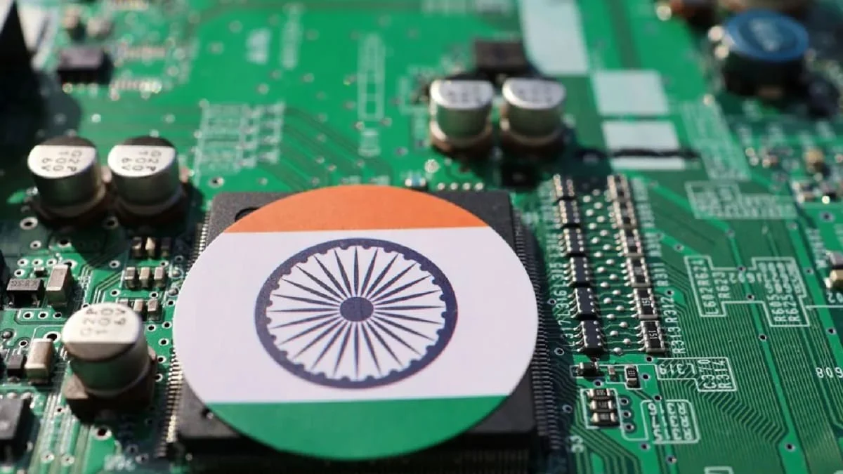
NEW DELHI, India – May 17, 2026 – In a landmark development poised to fundamentally reshape India’s technological landscape and cement its position in the global semiconductor arena, Tata Electronics, a wholly-owned subsidiary of the Indian conglomerate Tata Group, has formally inked a Memorandum of Understanding (MoU) with the Netherlands-based ASML. This strategic alliance with the world’s preeminent supplier of lithography equipment marks a pivotal moment for India’s burgeoning semiconductor manufacturing ecosystem, setting the stage for the establishment and successful ramp-up of Tata Electronics’ ambitious 300 mm (12-inch) semiconductor fabrication plant in Dholera, Gujarat.
The collaboration transcends a mere transactional agreement; it signifies a deep commitment to knowledge transfer, technological advancement, and the cultivation of a robust indigenous semiconductor industry. ASML, an undisputed titan whose sophisticated machinery is indispensable for producing nearly every advanced microchip globally, will deploy its "holistic suite of advanced lithography tools and solutions" to power the Dholera fab. This comprehensive support is critical, as ASML’s unique technological prowess, particularly in Extreme Ultraviolet (EUV) lithography – though the Dholera fab will initially focus on Deep Ultraviolet (DUV) for its specified nodes – makes it an irreplaceable partner for any nation aspiring to advanced chip manufacturing capabilities.
The Dholera facility, heralded as India’s inaugural planned commercial semiconductor fabrication plant, is envisioned to achieve a formidable monthly capacity of 50,000 wafers. These wafers will serve as the foundation for Analog and Logic IC chips, targeting technology nodes ranging from 28nm to 110nm – critical for a vast array of applications from automotive and industrial to consumer electronics and communication. With a planned total investment soaring to US$11 billion, this venture is a cornerstone of the India Semiconductor Mission (ISM), a national imperative aimed at transforming the subcontinent into a global manufacturing hub for advanced electronics.
A Chronology of India’s Semiconductor Aspirations
India’s ambition to establish a strong footprint in semiconductor manufacturing is not a recent phenomenon but rather a long-cherished dream punctuated by intermittent efforts and significant challenges. For decades, India has excelled in semiconductor design, boasting a substantial pool of highly skilled engineers contributing to global chip design houses. However, the absence of indigenous fabrication capabilities has rendered the nation dependent on imports, creating strategic vulnerabilities and economic outflows.
The current impetus gained significant momentum with the launch of the India Semiconductor Mission (ISM) in December 2021, under the aegis of the Ministry of Electronics and Information Technology (MeitY). The ISM outlined a comprehensive strategy, backed by a substantial financial outlay and production-linked incentive (PLI) schemes, to attract global players and foster domestic investment across the entire semiconductor value chain – from design and manufacturing to packaging and testing. The goal was clear: to reduce import dependency, enhance national security, and position India as a reliable participant in the global semiconductor supply chain diversification efforts.
Prior to the current wave, several attempts to set up fabs in India faced hurdles related to capital intensity, technology access, and policy consistency. However, the global semiconductor shortage exacerbated by the COVID-19 pandemic, coupled with rising geopolitical tensions, underscored the critical need for regionalized and diversified manufacturing capabilities. This global realignment created a fertile ground for India to aggressively pursue its semiconductor ambitions, with the government offering robust incentives and a conducive policy environment.
Tata Group, with its deep industrial roots and strategic foresight, emerged as a frontrunner in this national endeavor. Leveraging its vast resources and a long-term vision for high-tech manufacturing, Tata Electronics embarked on the Dholera project, strategically partnering with key global entities. A crucial early step was its alliance with Powerchip Semiconductor Manufacturing Corporation (PSMC) of Taiwan, a well-established foundry player, providing Tata Electronics access to a broad technology portfolio encompassing 28nm, 40nm, 55nm, 90nm, and 110nm processes. This initial partnership laid the technological groundwork, and the subsequent agreement with ASML now provides the indispensable equipment and expertise needed to bring these plans to fruition. The timeline, from the initial government incentives to the current ASML partnership, reflects a carefully orchestrated and accelerated push towards realizing India’s chip-making dreams.
Decoding the Partnership: ASML’s Indispensable Role and Tata’s Vision
The significance of ASML’s involvement cannot be overstated. In the intricate, capital-intensive, and technologically demanding world of semiconductor manufacturing, ASML occupies a unique and almost monopolistic position. It is the sole producer of Extreme Ultraviolet (EUV) lithography machines, the cutting-edge technology required to etch the minuscule features found in the most advanced chips powering AI, 5G, quantum computing, and high-performance computing. Even for less advanced nodes, ASML’s Deep Ultraviolet (DUV) lithography systems are industry benchmarks, renowned for their precision, reliability, and throughput.
Lithography, essentially the photographic process of printing circuit patterns onto silicon wafers, is the heart of chip manufacturing. The ability to shrink these patterns, enabling more transistors on a single chip, drives the exponential progress observed in computing power (Moore’s Law). ASML’s machines, a marvel of optics and engineering, are the keys to unlocking this miniaturization. Top-tier chip manufacturers globally, including giants like TSMC, Samsung Electronics, and Intel, are fundamentally reliant on ASML’s equipment to produce their chips. This dependence underscores ASML’s role as a critical "chokepoint" in the global semiconductor supply chain, making its partnerships highly coveted and strategically significant.
For Tata Electronics’ Dholera fab, ASML’s "holistic suite of advanced lithography tools and solutions" implies far more than just selling machines. It encompasses comprehensive support including:
- Equipment Installation and Calibration: Ensuring optimal performance of highly complex lithography systems.
- Process Integration Expertise: Guiding Tata engineers on how to integrate lithography steps seamlessly with other fabrication processes.
- Maintenance and Servicing: Providing specialized technicians and spare parts to ensure maximum uptime, crucial in a 24/7 manufacturing environment.
- Software and Control Systems: Supplying proprietary software that optimizes wafer processing and ensures quality control.
- Future Technology Roadmap: Offering insights and pathways for potential upgrades or transitions to more advanced nodes down the line, including eventual EUV readiness.
While the Dholera fab is initially targeting 28nm to 110nm nodes, which typically utilize DUV lithography, ASML’s expertise ensures that the foundation is laid for future scalability and technological advancement. Access to ASML’s advanced DUV systems and the accompanying technical know-how is paramount for achieving high yields and competitive performance at these nodes.
Tata Electronics’ vision for the Dholera fab is ambitious. The US$11 billion investment reflects not just the cost of advanced machinery but also the extensive infrastructure, research, and human capital development required. The plant’s focus on Analog and Logic IC chips for automotive, mobile devices, AI, and other key segments positions it to address rapidly growing global demand. The strategic partnership with PSMC provides the initial technology transfer, and ASML’s involvement elevates the project’s credibility and technological capability, enabling Tata to serve customers globally with a robust and competitive product portfolio.
Building an Ecosystem: Beyond Equipment
The partnership with ASML extends beyond the mere provision of machinery; it is a foundational element in building a sustainable and self-reliant semiconductor ecosystem in India. The joint press release explicitly highlights cooperation in three critical areas: domestic talent development, supply chain localization, and research initiatives.
1. Domestic Talent Development: The semiconductor industry is notoriously complex and demands a highly specialized workforce. India, while strong in software and IT services, has a nascent talent pool in hardware manufacturing, particularly in the intricacies of wafer fabrication. ASML’s involvement will be crucial in:
- Training Programs: Establishing specialized training modules and workshops for Indian engineers and technicians on operating and maintaining advanced lithography equipment.
- Skill Transfer: Facilitating knowledge transfer from ASML’s global experts to local teams, fostering a deep understanding of manufacturing processes and quality control.
- Academic Collaboration: Potentially partnering with Indian universities and research institutions to develop curricula tailored to semiconductor manufacturing, creating a pipeline of future talent. This includes areas like materials science, precision engineering, optics, and vacuum technology.
2. Supply Chain Localization: A thriving semiconductor fab requires a robust ecosystem of ancillary industries providing everything from ultra-pure chemicals, gases, and specialized materials to precision components, tools, and maintenance services. Relying solely on imports for these critical inputs creates vulnerabilities and increases costs. The collaboration aims to:
- Identify Local Suppliers: Working with Indian businesses to identify and develop local sources for consumables and components, thereby reducing import dependence.
- Quality Assurance: Guiding local suppliers to meet the stringent quality and purity standards required for semiconductor manufacturing.
- Logistics Optimization: Streamlining the supply chain within India to ensure timely and efficient delivery of materials to the Dholera fab. This will reduce lead times and improve overall operational efficiency.
3. Research & Development Initiatives: To remain competitive in the rapidly evolving semiconductor landscape, continuous innovation is essential. The partnership intends to foster local R&D capabilities by:
- Joint Research Projects: Collaborating on specific research challenges related to process optimization, material science, and yield improvement.
- Innovation Hubs: Potentially establishing R&D centers in India that can contribute to advancing lithography techniques or developing new applications for the chips produced.
- Future Technology Exploration: Preparing for the adoption of next-generation technologies, ensuring India stays abreast of global advancements.
By focusing on these three pillars, the Tata-ASML partnership aims to cultivate a self-sustaining ecosystem that can not only support the Dholera fab but also serve as a foundation for future semiconductor ventures in India.
Official Responses and Industry Perspectives
While specific direct quotes from the latest announcement are yet to be fully released, the tenor of such a high-profile partnership allows for informed inferences regarding official responses.
From the perspective of Tata Electronics, this partnership is likely viewed as a monumental step in realizing their vision for India’s technological future. A representative, perhaps the CEO, would likely emphasize the group’s unwavering commitment to building indigenous capabilities, stating something to the effect of: "This collaboration with ASML, a global leader and innovator, is a testament to Tata Electronics’ resolve to establish a world-class semiconductor manufacturing facility in India. It not only brings cutting-edge technology to our shores but also underscores our dedication to fostering local talent and strengthening India’s position in the global high-tech value chain."
ASML’s leadership would undoubtedly highlight their role as a critical enabler for global chip production and express confidence in India’s potential. A statement from an ASML executive might read: "ASML is proud to partner with Tata Electronics in this ambitious endeavor. Our commitment is to provide the comprehensive lithography solutions and expertise necessary to make the Dholera fab a success. We believe India possesses immense potential to become a significant player in semiconductor manufacturing, and we are excited to contribute to the development of its advanced technology ecosystem."
Indian government officials, particularly from MeitY and the India Semiconductor Mission, would hail this as a resounding success for the "Make in India" and "Atmanirbhar Bharat" (self-reliant India) initiatives. A ministerial statement would likely underscore the strategic importance: "The partnership between Tata Electronics and ASML is a game-changer for India’s semiconductor journey. It validates our policy framework, attracts critical technology, and accelerates our goal of becoming a reliable and indispensable hub in the global semiconductor supply chain. This will not only create high-skilled jobs but also fuel innovation across various sectors."
Industry analysts have largely reacted positively, viewing the ASML partnership as a significant de-risking factor for Tata’s fab project. "Securing ASML’s support is non-negotiable for any serious fabrication effort," remarked Dr. Anshul Gupta, a leading semiconductor industry analyst. "It provides instant credibility and access to unparalleled technical know-how. While 28nm isn’t the most advanced node, starting with it and having ASML’s backing is the right strategic move for India to build foundational capabilities and climb the technology ladder." Other analysts might point to the geopolitical implications, noting that such a partnership strengthens India’s strategic autonomy and diversifies the global semiconductor footprint.
Profound Implications for India’s Global Chip Ambition
The Tata-ASML partnership carries a multitude of profound implications, touching upon India’s strategic autonomy, economic growth, technological advancement, and geopolitical standing.
1. Strategic Autonomy and National Security:
Perhaps the most critical implication is the boost to India’s strategic autonomy. Semiconductors are the bedrock of modern technology, from defense systems and critical infrastructure to everyday consumer electronics. Dependence on foreign suppliers for these essential components creates significant vulnerabilities, especially in times of geopolitical tensions or trade disruptions. By establishing domestic fabrication capabilities with a global leader like ASML, India significantly reduces its reliance on imports, bolstering its national security and ensuring a resilient supply chain for critical technologies. This move is aligned with global efforts to diversify manufacturing away from single points of failure.
2. Economic Transformation and Job Creation:
The US$11 billion investment in the Dholera fab represents a massive injection into the Indian economy. Beyond the direct investment, the project is expected to create thousands of highly skilled jobs in engineering, manufacturing, R&D, and quality control. Furthermore, the development of a robust local supply chain will stimulate growth in ancillary industries, leading to indirect job creation across a wide spectrum of sectors, from chemicals and gases to precision tooling and logistics. This high-value manufacturing will contribute significantly to India’s GDP, attracting further foreign direct investment (FDI) and positioning India as an attractive destination for advanced manufacturing. The potential for exports of domestically manufactured chips will also boost India’s trade balance.
3. Technological Advancement and Innovation Ecosystem:
Access to ASML’s state-of-the-art lithography machines and expertise will accelerate India’s technological learning curve. It will expose Indian engineers and researchers to the most advanced manufacturing processes, fostering a culture of precision engineering, quality control, and continuous innovation. This partnership can serve as a catalyst for a broader innovation ecosystem, encouraging startups in semiconductor design, materials science, and equipment servicing. Over time, as India gains experience and expertise, it can potentially move towards manufacturing more advanced nodes, climbing the technological ladder and contributing to global breakthroughs.
4. Geopolitical Rebalancing and Supply Chain Diversification:
The global semiconductor supply chain has long been concentrated in a few key regions, particularly East Asia. This concentration has become a point of concern for major economies seeking to de-risk their technological dependencies. India’s entry into advanced chip manufacturing, backed by a player of ASML’s stature, contributes to the much-needed diversification of this critical supply chain. It positions India as a reliable and strategically important partner, strengthening its leverage in global technology dialogues and potentially attracting further investments from companies looking to establish resilient manufacturing footprints outside traditional hubs.
5. Challenges and the Road Ahead:
Despite the immense promise, the path to becoming a global chip hub is fraught with challenges. The semiconductor industry is characterized by its extreme capital intensity, rapid technological obsolescence, and fierce global competition.
- Sustained Government Support: Long-term and consistent policy support, including financial incentives, infrastructure development, and regulatory stability, will be crucial for the Dholera fab’s success.
- Talent Pipeline: While the partnership addresses talent development, ensuring a continuous supply of highly skilled engineers and technicians will require sustained investment in education and vocational training.
- Cost Competitiveness: India will need to maintain a competitive cost structure relative to established manufacturing hubs, balancing labor costs with efficiency and quality.
- Technological Evolution: The rapid pace of technological change means continuous investment in R&D and upgrades will be necessary to stay relevant. The journey from 28nm to sub-10nm nodes is complex and expensive.
- Global Competition: Other nations are also aggressively pursuing semiconductor manufacturing investments, creating a competitive landscape for attracting talent and capital.
Conclusion
The partnership between Tata Electronics and ASML represents a watershed moment in India’s quest to become a significant player in the global semiconductor landscape. It transcends a mere business deal, symbolizing a convergence of India’s national ambition with ASML’s unparalleled technological prowess. By securing access to the world’s most critical chipmaking equipment and expertise, India is not just building a factory; it is laying the foundation for a resilient, self-reliant, and technologically advanced future.
The Dholera fab, backed by substantial investment and strategic alliances, is poised to be a beacon of India’s "Make in India" vision, contributing significantly to its economic growth, job creation, and strategic autonomy. While challenges undoubtedly lie ahead, the commitment from both Tata and ASML, coupled with a supportive government policy, signals a determined leap forward. As the global demand for semiconductors continues to surge, India’s entry into advanced chip manufacturing is not just timely but strategically imperative, promising to redefine its role in the global technology order for decades to come.
