

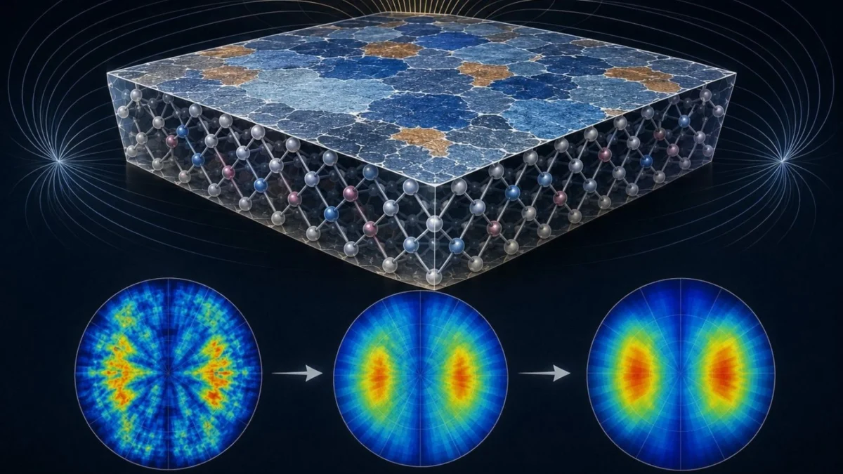
In a landmark study published in the journal PNAS, researchers have decoded the "quantum puddle" behavior of boron-doped diamonds, paving the way for monolithic "quantum-on-chip" architectures that could redefine the future of high-speed, energy-efficient computing.
For decades, the diamond has been celebrated as the "ultimate semiconductor" due to its unparalleled hardness, exceptional thermal conductivity, and wide bandgap. However, a new study released in May 2026 has shifted the focus from diamond’s structural resilience to its quantum potential. By peering into the microscopic world of heavily boron-doped diamonds, a global team of physicists has uncovered a complex, granular superconducting landscape that could bridge the gap between traditional microelectronics and next-generation quantum processors.
Main Facts: The Emergence of the "Quantum Puddle"
The central revelation of the research, published on May 11, 2026, in the Proceedings of the National Academy of Sciences (PNAS), is the discovery of "intrinsic electronic granularity" within diamond films. While diamond is naturally a near-perfect insulator, the introduction of boron atoms—a process known as doping—replaces carbon atoms in the lattice and introduces "holes" (positive charge carriers).
When boron concentration reaches a critical threshold, the diamond undergoes a phase transition, transforming into a superconductor capable of carrying electricity with zero resistance. However, the 2026 study reveals that this transition is far from uniform. Instead of the entire film becoming a superconductor simultaneously, the material develops "quantum puddles"—tiny, localized regions of superconductivity—embedded within a metallic matrix.
Key findings from the report include:
- Transition Threshold: Superconductivity begins to emerge at a critical temperature of approximately 3.3 Kelvin (-269.85°C).
- Granular Nature: The material does not behave as a homogenous block; rather, superconducting islands expand and eventually coalesce as temperatures drop.
- Magnetic Sensitivity: The superconducting state is highly sensitive to external magnetic fields, showing unique resistance patterns when fields are rotated in three dimensions.
- Structural Control: The use of Microwave Plasma Chemical Vapour Deposition (MPCVD) allowed researchers to achieve unprecedented precision in boron distribution.
Chronology: The Road to Diamond Superconductivity
The journey toward the 2026 breakthrough has been over two decades in the making. To understand the significance of this discovery, one must look at the timeline of diamond research:
2004: The Ekimov Breakthrough
The scientific community was first stunned in 2004 when a team led by Alexei Ekimov at the Institute for High Pressure Physics in Russia discovered superconductivity in synthetic diamond. Using high-pressure, high-temperature (HPHT) synthesis, they found that diamond could superconduct at 2.3 Kelvin. This shattered the long-held belief that diamond was strictly an insulator.
2005–2015: The Quest for Quality
Following the 2004 discovery, researchers struggled with the "disorder" problem. HPHT synthesis often resulted in uneven boron distribution, making it difficult to study the underlying physics. During this decade, the focus shifted toward Chemical Vapour Deposition (CVD), which allowed for the growth of high-purity thin films.
2016–2024: Quantum Sensing and NV Centers
As the "Quantum Race" intensified, scientists focused on Nitrogen-Vacancy (NV) centers in diamonds for use as quantum bits (qubits) and sensors. However, the integration of these qubits with superconducting circuits remained a challenge because the two components usually required different materials and manufacturing processes.
May 2026: The PNAS Publication
The current study marks the culmination of these efforts. By utilizing advanced MPCVD techniques and cryogenic transport measurements, the research team finally mapped the "granularity" of the boron-doped diamond. This provided the first clear explanation of how superconductivity survives and spreads through a disordered crystal lattice.
Supporting Data: Cryogenic Transport and 3D Magnetic Mapping
The researchers utilized a suite of high-precision instruments to validate their findings. The data gathered during the experiment provides a detailed look at how the "quantum puddles" interact.
1. Temperature-Dependent Resistance
The team observed that as the temperature decreased toward 3.3 Kelvin, the electrical resistance of the boron-doped diamond began a sharp decline. Unlike "clean" superconductors that show a near-instantaneous drop to zero, the diamond films showed a multi-stage transition. This "smearing" of the resistance curve is a classic signature of granularity, where different "puddles" reach the superconducting state at slightly different temperatures.
2. 3D Magnetic Field Rotation
To probe the limits of these superconducting regions, the scientists subjected the films to powerful magnetic fields. By rotating the magnetic field vector in three dimensions (x, y, and z axes), they mapped the material’s anisotropy. They found that the superconductivity was more resilient in certain orientations, suggesting that the "puddles" are shaped by the specific growth planes of the diamond crystal.
3. Microwave Plasma Chemical Vapour Deposition (MPCVD)
The films were grown using MPCVD, a process where a plasma of methane and hydrogen is used to deposit carbon atoms onto a substrate. By introducing diborane gas into the plasma, boron atoms are "sprinkled" into the growing diamond. The data showed that a boron concentration of roughly $10^21$ atoms per cubic centimeter was necessary to trigger the granular superconducting state.
Official Responses: The Scientific Community Reacts
The implications of the study have drawn praise from both academia and the burgeoning quantum computing industry. While the lead researchers remain cautious about immediate commercialization, their outlook is overwhelmingly positive.
The Research Team’s Perspective:
In a statement accompanying the study, the lead authors noted: "Our findings resolve a long-standing debate in condensed matter physics regarding the nature of superconductivity in doped semiconductors. By identifying the ‘intrinsic electronic granularity,’ we now have a roadmap for engineering diamond films with specific quantum properties."
Industry Analysts:
Tech analysts suggest that this research could be the "missing link" for scalable quantum hardware. "The ability to have superconductivity and semiconductivity in the same material—diamond—is a game-changer," says Dr. Elena Vance, a senior quantum hardware consultant. "It eliminates the ‘interface noise’ that occurs when you try to connect different materials like silicon and aluminum in a quantum processor."
Condensed Matter Physicists:
Theoretical physicists have highlighted the study’s contribution to understanding "multifractal superconductivity." This is a rare state where the quantum wave functions of electrons exhibit fractal patterns. The PNAS study provides some of the strongest experimental evidence to date that boron-doped diamond is a candidate for observing these exotic states of matter.
Implications: The "Quantum-on-Chip" Future
The discovery of how superconductivity behaves in diamond has profound implications for the future of technology, moving beyond theoretical physics into practical engineering.
1. Monolithic Quantum Platforms
Currently, quantum computers are "hybrid" machines. They use one material for qubits (like trapped ions or superconducting circuits) and another for the surrounding electronics. This creates massive engineering hurdles in terms of thermal expansion and signal loss.
The 2026 study suggests a future where a single diamond chip could be "zoned":
- Zone A: Pure diamond for high-speed thermal management.
- Zone B: Boron-doped superconducting pathways for lossless data transmission.
- Zone C: NV-center sites for quantum memory and processing.
2. Extreme Environment Computing
Because diamond is incredibly stable, diamond-based quantum chips could theoretically operate in environments that would destroy silicon-based electronics. This includes high-radiation environments like outer space or high-temperature industrial settings, although the superconducting elements would still require cryogenic cooling.
3. Energy Efficiency and Heat Dissipation
One of the greatest bottlenecks in modern computing is heat. Diamond has the highest thermal conductivity of any known bulk material. By using superconducting diamond pathways, heat generation is virtually eliminated in the "puddles," and any residual heat from other components is dissipated almost instantly by the diamond substrate.
4. Advancing the "Pseudogap" Debate
The study also touches on the "pseudogap" state—a mysterious phase where a material shows some characteristics of a superconductor but lacks zero resistance. Understanding this in diamond could help scientists unlock the secrets of high-temperature superconductivity in other materials, such as cuprates, potentially leading to superconductors that work at room temperature.
Conclusion: The Long Road to the Diamond Age
While the PNAS study is a monumental step forward, the researchers emphasize that a "Diamond Quantum Computer" is not hitting shelves next year. The requirement for temperatures near absolute zero (3.3 Kelvin) remains a significant barrier for consumer use. Furthermore, scaling the MPCVD process to produce large-scale, perfectly uniform doped films remains an industrial challenge.
However, the 2026 discovery has provided the most detailed "blueprints" yet for the internal life of a superconducting diamond. By understanding the "quantum puddles," scientists have stopped guessing and started engineering. As the world moves toward a post-silicon era, the diamond is no longer just a girl’s best friend—it may very well be the best friend of the quantum engineer.
Article Information:
- Source Material: PNAS Journal, May 11, 2026.
- Subject: Boron-doped diamond (BDD) superconductivity.
- Key Terms: Cryogenic transport, MPCVD, Quantum Puddles, Multifractality.
- Date of Report: May 26, 2026.
